- 您现在的位置:买卖IC网 > Sheet目录1998 > ICS874001AGI-02LF (IDT, Integrated Device Technology Inc)IC PCI EXPRSS/JITT ATTEN 20TSSOP
ICS874001AGI-02 REVISION A AUGUST 30, 2010
12
2010 Integrated Device Technology, Inc.
ICS74001I-02 Data Sheet
PCI EXPRESS JITTER ATTENUATOR
Recommendations for Unused Input Pins
Inputs:
LVCMOS Control Pins
All control pins have internal pull-ups or pull-downs; additional
resistance is not required but can be added for additional protection.
A 1k
resistor can be used.
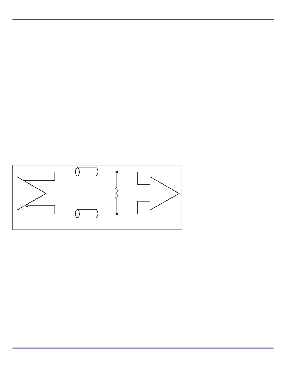
LVDS Driver Termination
A general LVDS interface is shown in Figure 4. Standard termination
for LVDS type output structure requires both a 100
parallel resistor
at the receiver and a 100
differential transmission line environment.
In order to avoid any transmission line reflection issues, the 100
resistor must be placed as close to the receiver as possible. IDT
offers a full line of LVDS compliant devices with two types of output
structures: current source and voltage source. The standard
termination schematic as shown in Figure 4 can be used with either
type of output structure. If using a non-standard termination, it is
recommended to contact IDT and confirm if the output is a current
source or a voltage source type structure. In addition, since these
outputs are LVDS compatible, the amplitude and common mode
input range of the input receivers should be verified for compatibility
with the output.
Figure 4. Typical LVDS Driver Termination
100
–
+
100
Differential Transmission Line
LVDS Driver
LVDS
Receiver
发布紧急采购,3分钟左右您将得到回复。
相关PDF资料
ICS874001AGI-05LFT
IC PCI EXPRSS/JITT ATTEN 20TSSOP
ICS874002AGLFT
IC PCI EXPRSS/JITT ATTEN 20TSSOP
ICS874005AG-04LFT
IC PCI EXPRSS/JITT ATTEN 24TSSOP
ICS874005AGLFT
IC PCI EXPRSS/JITT ATTEN 24TSSOP
ICS8741004AGLFT
IC PCI EXPRSS/JITT ATTEN 24TSSOP
ICS87604AGILF
IC CLK MULT/ZD BUFFER 28-TSSOP
ICS8761CYLFT
IC CLK GEN PCI/PCI-X 64-LQFP
ICS87946AYILFT
IC CLOCK GENERATOR 32-LQFP
相关代理商/技术参数
ICS874001AGI-02LFT
功能描述:IC PCI EXPRSS/JITT ATTEN 20TSSOP RoHS:是 类别:集成电路 (IC) >> 时钟/计时 - 专用 系列:FemtoClock™, PCI Express™ (PCIe) 标准包装:1,500 系列:- 类型:时钟缓冲器/驱动器 PLL:是 主要目的:- 输入:- 输出:- 电路数:- 比率 - 输入:输出:- 差分 - 输入:输出:- 频率 - 最大:- 电源电压:3.3V 工作温度:0°C ~ 70°C 安装类型:表面贴装 封装/外壳:28-SSOP(0.209",5.30mm 宽) 供应商设备封装:28-SSOP 包装:带卷 (TR) 其它名称:93786AFT
ICS874001AGI-05LF
功能描述:IC PCI EXPRSS/JITT ATTEN 20TSSOP RoHS:是 类别:集成电路 (IC) >> 时钟/计时 - 专用 系列:FemtoClock™, PCI Express™ (PCIe) 标准包装:1 系列:- 类型:时钟/频率发生器,多路复用器 PLL:是 主要目的:存储器,RDRAM 输入:晶体 输出:LVCMOS 电路数:1 比率 - 输入:输出:1:2 差分 - 输入:输出:无/是 频率 - 最大:400MHz 电源电压:3 V ~ 3.6 V 工作温度:0°C ~ 85°C 安装类型:表面贴装 封装/外壳:16-TSSOP(0.173",4.40mm 宽) 供应商设备封装:16-TSSOP 包装:Digi-Reel® 其它名称:296-6719-6
ICS874001AGI-05LFT
功能描述:IC PCI EXPRSS/JITT ATTEN 20TSSOP RoHS:是 类别:集成电路 (IC) >> 时钟/计时 - 专用 系列:FemtoClock™, PCI Express™ (PCIe) 标准包装:1,500 系列:- 类型:时钟缓冲器/驱动器 PLL:是 主要目的:- 输入:- 输出:- 电路数:- 比率 - 输入:输出:- 差分 - 输入:输出:- 频率 - 最大:- 电源电压:3.3V 工作温度:0°C ~ 70°C 安装类型:表面贴装 封装/外壳:28-SSOP(0.209",5.30mm 宽) 供应商设备封装:28-SSOP 包装:带卷 (TR) 其它名称:93786AFT
ICS874002AGLF
功能描述:IC JITTER ATTENUATOR 20-TSSOP RoHS:是 类别:集成电路 (IC) >> 时钟/计时 - 专用 系列:HiPerClockS™, PCI Express® (PCIe) 标准包装:1 系列:- 类型:时钟/频率发生器,多路复用器 PLL:是 主要目的:存储器,RDRAM 输入:晶体 输出:LVCMOS 电路数:1 比率 - 输入:输出:1:2 差分 - 输入:输出:无/是 频率 - 最大:400MHz 电源电压:3 V ~ 3.6 V 工作温度:0°C ~ 85°C 安装类型:表面贴装 封装/外壳:16-TSSOP(0.173",4.40mm 宽) 供应商设备封装:16-TSSOP 包装:Digi-Reel® 其它名称:296-6719-6
ICS874002AGLFT
功能描述:IC PCI EXPRSS/JITT ATTEN 20TSSOP RoHS:是 类别:集成电路 (IC) >> 时钟/计时 - 专用 系列:HiPerClockS™, PCI Express® (PCIe) 标准包装:1,500 系列:- 类型:时钟缓冲器/驱动器 PLL:是 主要目的:- 输入:- 输出:- 电路数:- 比率 - 输入:输出:- 差分 - 输入:输出:- 频率 - 最大:- 电源电压:3.3V 工作温度:0°C ~ 70°C 安装类型:表面贴装 封装/外壳:28-SSOP(0.209",5.30mm 宽) 供应商设备封装:28-SSOP 包装:带卷 (TR) 其它名称:93786AFT
ICS874003AG-02LF
功能描述:IC JITTER ATTENUATOR 20-TSSOP RoHS:是 类别:集成电路 (IC) >> 时钟/计时 - 专用 系列:HiPerClockS™, FemtoClock™, PCI Express® (PCIe) 标准包装:1 系列:- 类型:时钟/频率发生器,多路复用器 PLL:是 主要目的:存储器,RDRAM 输入:晶体 输出:LVCMOS 电路数:1 比率 - 输入:输出:1:2 差分 - 输入:输出:无/是 频率 - 最大:400MHz 电源电压:3 V ~ 3.6 V 工作温度:0°C ~ 85°C 安装类型:表面贴装 封装/外壳:16-TSSOP(0.173",4.40mm 宽) 供应商设备封装:16-TSSOP 包装:Digi-Reel® 其它名称:296-6719-6
ICS874003AG-02LFT
功能描述:IC PCI EXPRSS/JITT ATTEN 20TSSOP RoHS:是 类别:集成电路 (IC) >> 时钟/计时 - 专用 系列:HiPerClockS™, FemtoClock™, PCI Express® (PCIe) 标准包装:1,500 系列:- 类型:时钟缓冲器/驱动器 PLL:是 主要目的:- 输入:- 输出:- 电路数:- 比率 - 输入:输出:- 差分 - 输入:输出:- 频率 - 最大:- 电源电压:3.3V 工作温度:0°C ~ 70°C 安装类型:表面贴装 封装/外壳:28-SSOP(0.209",5.30mm 宽) 供应商设备封装:28-SSOP 包装:带卷 (TR) 其它名称:93786AFT
ICS874003AG-04LF
功能描述:IC PCI EXPRSS/JITT ATTEN 20TSSOP RoHS:是 类别:集成电路 (IC) >> 时钟/计时 - 专用 系列:HiPerClockS™, FemtoClock™, PCI Express® (PCIe) 标准包装:1,500 系列:- 类型:时钟缓冲器/驱动器 PLL:是 主要目的:- 输入:- 输出:- 电路数:- 比率 - 输入:输出:- 差分 - 输入:输出:- 频率 - 最大:- 电源电压:3.3V 工作温度:0°C ~ 70°C 安装类型:表面贴装 封装/外壳:28-SSOP(0.209",5.30mm 宽) 供应商设备封装:28-SSOP 包装:带卷 (TR) 其它名称:93786AFT